Sunday, March 25, 2012

global system for mobile application (GSM) controlled robot


Here, i m present  one of the advantage  of mobile  .hence  all the mobile keypad having there separate  tone dtmf(dual tone multiplexing frequency) on the basis of it we construct gsm controller.
.


complete circuit diagram given below ,we are using dtmf receiver ic (ht9170) to download  datasheet .


To download    atmega8 datasheet  .

  
to download  motor driver ic data sheet.

copy paste below code in notepad and give extension (.HEX) and load in your Atmega8Lplz do not miss code otherwise it's not working.


:1000000012C019C018C017C016C015C014C013C044
:1000100012C011C010C00FC00EC00DC00CC00BC06C
:100020000AC009C008C011241FBECFE5D4E0DEBF5E
:10003000CDBF02D02AC0E4CF8FEF87BB14BA6AE0ED
:1000400056E048E031E029E083B390E08F70907093
:100050008130910511F468BBF7CF8230910511F41E
:1000600028BBF2CF8430910511F438BBEDCF853039
:10007000910511F418BAE8CF8630910511F448BB08
:0E008000E3CF089709F758BBDFCFF894FFCF06
:00000001FF


here in mobile key pad  u can press key for above code  to control motor,

press 2 to going forward direction,
press 4 to going  left direction,
press 6 to going right direction,
press 8 to going backward,
press 5 to stop direction.

Friday, February 10, 2012

Line Follower Bot Using Controller

Here ,i m give the code of line follower in assembly language .  we are loaded  this in 89v51rd2 NXP  .


ORG 0000H
SETB P1.6                             ; CONFIG P1.6 AS I/P PIN
MOV C,P1.6                        ; I HAVE CONNECTED A S/W HERE TO START THE ROBOT
JC STOP
MOV P3,#3CH                   ;4 SENSOR INPUTS ARE CONNECTED AT P3.5,P3.4,P3.3 AND P3.2
MOV P1,#00H                    ;CONFIG AS O/P PORT
CLR A
AGAIN: MOV A,P3
ORL  A,#14H                       ; CHECK IF FRONT OR BACK SENSOR ARE ON
JB P3.3,CHECK_LEFT        ; CHECK IF LEFT SIDE SENSOR IS ON
JB P3.5,CHECK_RIGHT    ; CHECK IF RIGHT SIDE SENSOR IS ON
CJNE A,#14H,STOP          ; CHECK IF FRONT ON BACK SENSOR ARE ON
SETB P1.1                             ;ENABLE 2 OF L293D MOTOR DRIVER IC
SETB P1.2                             ;ROTATE RIGHT MOTOR IN CLOCKWISE DIRECTION
SETB P1.3                             ;ROTATE RIGHT MOTOR IN CLOCKWISE DIRECTION
SETB P1.4                             ;ROTATE LEFT MOTOR IN CLOCKWISE DIRECTION
CLR P1.5                               ;ROTATE LEFT MOTOR IN CLOCKWISE DIRECTION
AJMP AGAIN

CHECK_LEFT:
MOV A,P3
ANL A, #08H
CJNE A,#08H,AGAIN       ;RECHECK IF LEFT SIDE SENSOR IS ON
SETB P1.0                             ; ENABLE 1 OF L293D MOTOR DRIVER IC
SETB P1.1                             ;ENABLE 2 OF L293D MOTOR DRIVER IC
SETB P1.2                             ;ROTATE RIGHT MOTOR IN CLOCKWISE DIRECTION
CLR P1.3                               ;ROTATE RIGHT MOTOR IN CLOCKWISE DIRECTION
CLR P1.4                               ;ROTATE LEFT MOTOR IN ANTICLOCKWISE DIRECTION
SETB P1.5                             ;ROTATE LEFT MOTOR IN ANTICLOCKWISE DIRECTION
ACALL DELAY
AJMP AGAIN

CHECK_RIGHT:
MOV A,P3
ANL A, #20H
CJNE A,#20H,AGAIN       ;RECHECK IF LEFT SIDE SENSOR IS ON
SETB P1.0                             ; ENABLE 1 OF L293D MOTOR DRIVER IC
SETB P1.1                             ;ENABLE 2 OF L293D MOTOR DRIVER IC
CLR P1.2                               ;ROTATE RIGHT MOTOR IN ANTICLOCKWISE DIRECTION
SETB P1.3                             ;ROTATE RIGHT MOTOR IN ANTICLOCKWISE DIRECTION
SETB P1.4                             ;ROTATE LEFT MOTOR IN CLOCKWISE DIRECTION
CLR P1.5                               ;ROTATE LEFT MOTOR IN CLOCKWISE DIRECTION
ACALL DELAY
AJMP AGAIN

DELAY:
CLR TF0
MOV R0,#14H
L1: MOV TL0,#00H
MOV TH0, #4CH
CLR TR0
L2: JNB TF0,L2
CLR TR0
CLR TF0
DJNZ R0,L1
RET

STOP:
MOV A,P3
ANL A, #3CH
CJNE A,#00H,AGAIN       ; RE-RCHECK IF ANY SENSOR ON
SETB P1.2                             ; STOP RIGHT MOTOR
SETB P1.3                             ; STOP RIGHT MOTOR
SETB P1.4                             ; STOP LEFT MOTOR
SETB P1.5                             ; STOP LEFT MOTOR
END.


Now  i  m introduced with interfacing of sensor ,their layout  given below ,

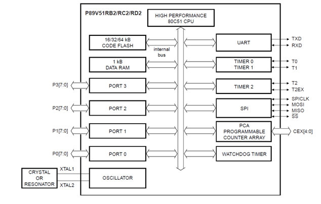
Block diagram of 89v51rd2.:


pin diagram :


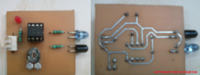
HERE WE   INTERFACE 6 SENSOR  AND SENSOR DIAGRAM PCB AND SCHMATIC GIVEN BELOW  USING LM358(LOW POWER DUAL OPERATIONAL AMPLIFIERS)
PCB LAYOUT OF LINE FOLLOWER FROM BOTTTOM (SOLDER SIDE) AND UPPER SIDE IS GIVEN IN FIG.


SENSOR PCB LAYOUT OF UPPER SIDE AND SOLDER SIDE (BOTTOM SIDE)


Robotics Fundamentals Of Death | Idea | Trick. IIT 2012

ROBO WAR :


ROBO WAR FINAL ROUND @IIT 2012 BOMBAY


IC ENGINE:-