Saturday, January 31, 2015

How to make wireless robot car !!!!

Here,i m introduced wireless robo car using encoder(ht12e), decoder(ht12d) (ic) and RF modual  (433 MHz).here  i m using l298 dual full bridge driver ic .it having 1A current source  capability .
Now basic concept of wireless is  transmit the information through the transmitter and receive these information through  receiver  but  first  communicate with each other  synchronization is required  between transmitter and receiver so i m  using dip switch .through which i m adjust  the code same in both Tx and Rx.


here, i am give you  DPDT switch  configuration in remote control .


Now ,pin diagram of ht12e and ht12d ic   given below ,


For HT12d ,


Now ,main circuit diagram of transmitter and receiver circuit  is  given below .


Tx


Rx


l298 to view clik here

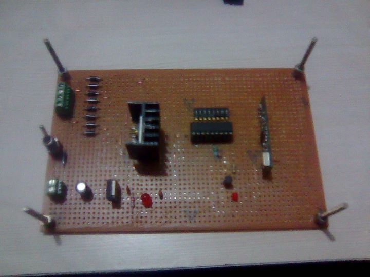
 After implement your component in PCB  is look like


uhhhhhhh!!!   now  your  wireless robo car  ready to drive
Let's   go on long  car drive  with your  GF......:) enjoyyyyy...

Sunday, March 25, 2012

global system for mobile application (GSM) controlled robot


Here, i m present  one of the advantage  of mobile  .hence  all the mobile keypad having there separate  tone dtmf(dual tone multiplexing frequency) on the basis of it we construct gsm controller.
.


complete circuit diagram given below ,we are using dtmf receiver ic (ht9170) to download  datasheet .


To download    atmega8 datasheet  .

  
to download  motor driver ic data sheet.

copy paste below code in notepad and give extension (.HEX) and load in your Atmega8Lplz do not miss code otherwise it's not working.


:1000000012C019C018C017C016C015C014C013C044
:1000100012C011C010C00FC00EC00DC00CC00BC06C
:100020000AC009C008C011241FBECFE5D4E0DEBF5E
:10003000CDBF02D02AC0E4CF8FEF87BB14BA6AE0ED
:1000400056E048E031E029E083B390E08F70907093
:100050008130910511F468BBF7CF8230910511F41E
:1000600028BBF2CF8430910511F438BBEDCF853039
:10007000910511F418BAE8CF8630910511F448BB08
:0E008000E3CF089709F758BBDFCFF894FFCF06
:00000001FF


here in mobile key pad  u can press key for above code  to control motor,

press 2 to going forward direction,
press 4 to going  left direction,
press 6 to going right direction,
press 8 to going backward,
press 5 to stop direction.

Friday, February 10, 2012

Line Follower Bot Using Controller

Here ,i m give the code of line follower in assembly language .  we are loaded  this in 89v51rd2 NXP  .


ORG 0000H
SETB P1.6                             ; CONFIG P1.6 AS I/P PIN
MOV C,P1.6                        ; I HAVE CONNECTED A S/W HERE TO START THE ROBOT
JC STOP
MOV P3,#3CH                   ;4 SENSOR INPUTS ARE CONNECTED AT P3.5,P3.4,P3.3 AND P3.2
MOV P1,#00H                    ;CONFIG AS O/P PORT
CLR A
AGAIN: MOV A,P3
ORL  A,#14H                       ; CHECK IF FRONT OR BACK SENSOR ARE ON
JB P3.3,CHECK_LEFT        ; CHECK IF LEFT SIDE SENSOR IS ON
JB P3.5,CHECK_RIGHT    ; CHECK IF RIGHT SIDE SENSOR IS ON
CJNE A,#14H,STOP          ; CHECK IF FRONT ON BACK SENSOR ARE ON
SETB P1.1                             ;ENABLE 2 OF L293D MOTOR DRIVER IC
SETB P1.2                             ;ROTATE RIGHT MOTOR IN CLOCKWISE DIRECTION
SETB P1.3                             ;ROTATE RIGHT MOTOR IN CLOCKWISE DIRECTION
SETB P1.4                             ;ROTATE LEFT MOTOR IN CLOCKWISE DIRECTION
CLR P1.5                               ;ROTATE LEFT MOTOR IN CLOCKWISE DIRECTION
AJMP AGAIN

CHECK_LEFT:
MOV A,P3
ANL A, #08H
CJNE A,#08H,AGAIN       ;RECHECK IF LEFT SIDE SENSOR IS ON
SETB P1.0                             ; ENABLE 1 OF L293D MOTOR DRIVER IC
SETB P1.1                             ;ENABLE 2 OF L293D MOTOR DRIVER IC
SETB P1.2                             ;ROTATE RIGHT MOTOR IN CLOCKWISE DIRECTION
CLR P1.3                               ;ROTATE RIGHT MOTOR IN CLOCKWISE DIRECTION
CLR P1.4                               ;ROTATE LEFT MOTOR IN ANTICLOCKWISE DIRECTION
SETB P1.5                             ;ROTATE LEFT MOTOR IN ANTICLOCKWISE DIRECTION
ACALL DELAY
AJMP AGAIN

CHECK_RIGHT:
MOV A,P3
ANL A, #20H
CJNE A,#20H,AGAIN       ;RECHECK IF LEFT SIDE SENSOR IS ON
SETB P1.0                             ; ENABLE 1 OF L293D MOTOR DRIVER IC
SETB P1.1                             ;ENABLE 2 OF L293D MOTOR DRIVER IC
CLR P1.2                               ;ROTATE RIGHT MOTOR IN ANTICLOCKWISE DIRECTION
SETB P1.3                             ;ROTATE RIGHT MOTOR IN ANTICLOCKWISE DIRECTION
SETB P1.4                             ;ROTATE LEFT MOTOR IN CLOCKWISE DIRECTION
CLR P1.5                               ;ROTATE LEFT MOTOR IN CLOCKWISE DIRECTION
ACALL DELAY
AJMP AGAIN

DELAY:
CLR TF0
MOV R0,#14H
L1: MOV TL0,#00H
MOV TH0, #4CH
CLR TR0
L2: JNB TF0,L2
CLR TR0
CLR TF0
DJNZ R0,L1
RET

STOP:
MOV A,P3
ANL A, #3CH
CJNE A,#00H,AGAIN       ; RE-RCHECK IF ANY SENSOR ON
SETB P1.2                             ; STOP RIGHT MOTOR
SETB P1.3                             ; STOP RIGHT MOTOR
SETB P1.4                             ; STOP LEFT MOTOR
SETB P1.5                             ; STOP LEFT MOTOR
END.


Now  i  m introduced with interfacing of sensor ,their layout  given below ,

Block diagram of 89v51rd2.:


pin diagram :


HERE WE   INTERFACE 6 SENSOR  AND SENSOR DIAGRAM PCB AND SCHMATIC GIVEN BELOW  USING LM358(LOW POWER DUAL OPERATIONAL AMPLIFIERS)
PCB LAYOUT OF LINE FOLLOWER FROM BOTTTOM (SOLDER SIDE) AND UPPER SIDE IS GIVEN IN FIG.


SENSOR PCB LAYOUT OF UPPER SIDE AND SOLDER SIDE (BOTTOM SIDE)


Robotics Fundamentals Of Death | Idea | Trick. IIT 2012

ROBO WAR :


ROBO WAR FINAL ROUND @IIT 2012 BOMBAY


IC ENGINE:-


Thursday, December 22, 2011

Charging Your Cell Phone | Home Made Circuit


For the cell phone to charge, charger output must be above 4V and can deliver a maximum current of 500mA. This charger circuit will step up the voltage from 1.5V to 5V DC to reach the cell phone charging requirement. The circuit uses only an AA or AAA 1.5v battery (1V to 2.4V). The charger is composed of simple oscillator, a rectifier, and voltage regulator. The feedback winding F is composed 5 turns of #30 AWG magnetic wire and main winding P is composed of 6 turns of #24 AWG wire. The 5.1V zener diode and 2200uF capacitor regulates the output voltage to ensure proper charging.

The windings are not critical, you can experiment using different number of turns. If ever the charger doesn’t have any output, try to reverse the winding connection.

Note:This charger is functional but provides not warranty on its accuracy. Try building at your own risk.

Variable Power Supply upto 30 volts @1.5A

Circuit Description:
In this circuit we are using transformer has capacity of 24 volt and 2 A current capacity that given at the output. Using bridge rectifier converts AC into DC and capacitor used for getting smooth dc voltage .LED used for indicate the power in the circuit the current through the led will be between 12 - 20mA at 2V depending on the type and color Led you are using. then smooth dc voltage apply to input terminal of voltage regulated IC LM317.variable resistor of 5 kilo ohm at adjust terminal of IC we can vary the voltage from 1.5v to 30 v .it is getting at the output terminal of IC .diode D1 is used as rectifier to block the current to flow in opposite direction. It steers any current that might be coming from the device under power around the regulator to prevent the regulator from being damaged Capacitor C2 used to filter any type of noise .also we use heat sink for IC because IC is heated during running of project. Maximum current is about 1.5 amps which is also sufficient for most of your tinkering. The large value of C1 makes for a good, low ripple output voltage. C2 is a 0.1µF (100nF) decoupler capacitor to filter out the transient noise which can be induced into the supply by stray magnetic fields. Under normal conditions this capacitor is only required if the regulator is far away from the filter cap, but I added it anyway. C3 improves transient response. This means that while the regulator may perform perfectly at DC and at low frequencies, (regulating the voltage regardless of the load current); at higher frequencies it may be less effective. Adding this 1 µF capacitor should improve the response at those frequencies.


APPLICATIONS INFORMATION LM 317
IC LM-317 (VOLTAGE REGULATED) DESCRIPTION:
The LM317 is an adjustable 3–terminal positive voltage regulator
Capable of supplying in excess of 1.5 a over an output voltage range of
1.2 V to 37 V. This voltage regulator is exceptionally easy to use and
Requires only two external resistors to set the output voltage
• Output Current in Excess of 1.5 A
• Output Adjustable between 1.2 V and 37 V
• Internal Thermal Overload Protection
• Internal Short Circuit Current Limiting Constant with Temperature
• Output Transistor Safe–Area Compensation
• Floating Operation for High Voltage Applications
• Available in Surface Mount D2PAK, and Standard 3–Lead Transistor
Package
• Eliminates stocking many Fixed Voltages
• C1 is required if regulator is located an appreciable distance from power supply filter.
• C2 is not needed for stability; however, it does improve transient response.
Features
• Guaranteed 1% output voltage tolerance
(LM317A)
• Y Guaranteed max. 0.01%/V line regulation
• (LM317A)
• Guaranteed max. 0.3% load regulation
(LM117)
• Guaranteed 1.5A output current
• Adjustable output down to 1.2V
• Current limit constant with temperature
• Pa Product Enhancement tested
• 80 dB ripple rejection
• Output is short-circuit protect.

Basic Circuit Operation:-

The LM317 is a 3–terminal floating regulator. In Operation, the LM317 develops and maintains a nominal 1.25 V reference (Vref) between its output and adjustment Terminals. This reference voltage is converted to a programming current (IPROG) by R1 and this Constant current flows through R2 to ground. The regulated output voltage is given by:

Since the current from the adjustment terminal (IAdj) represents an error term in the equation, the LM317 was designed to control IAdj to less than 100 mA and keep it constant. To do this, all quiescent operating current is returned to the output terminal. This imposes the requirement for a minimum load current. If the load current is less than this minimum, the output voltage will rise. Since the LM317 is a floating regulator, it is only the voltage differential across the circuit which is important to performance, and operation at high voltages with respect to
Ground is possible

Protection Diodes:-

When external capacitors are used with any IC regulator it is sometimes necessary to add protection diodes to prevent the capacitors from discharging through low current points into the regulator the LM317 with the recommended protection diodes for output voltages in excess of 25 V or high capacitance values (CO > 25 mF, CAdj > 10 mF). Diode D1 prevents CO from discharging thru the IC during an input short circuit. Diode D2 protects against capacitor CAdj discharging through the IC during an output short circuit. The combination of diodes D1 and D2 prevents CAdj from discharging through the IC during an input short circuit

External Capacitors:-
An input bypass capacitor is recommended. A 0.1 mF disc or 1 mF solid tantalum on the input is suitable input bypassing for almost all applications. The device is more sensitive
To the absence of input bypassing when adjustment or output capacitors are used but the above values will eliminate the possibility of problems. The adjustment terminal can be bypassed to ground on the LM117 to improve ripple rejection. This bypass capacitor
Prevents ripple from being amplified as the output voltage is increased. With a 10 mF bypass capacitor 80 dB ripple rejection is obtainable at any output level. Increases over 10 mF do not appreciably improve the ripple rejection at frequencies above 120 Hz. If the bypass capacitor is used, it is sometimes necessary to include protection diodes to prevent the capacitor from discharging through internal low current paths and damaging the device.
Load Regulation:-
The LM317 is capable of providing extremely good load regulation, but a few precautions are needed to obtain maximum performance. For best performance, the programming resistor (R1) should be connected as close to the regulator as possible to minimize line drops which effectively appear in series with the reference, thereby degrading regulation. The ground end of R2 can be returned near the load ground to provide remote ground sensing and improve load regulation

Wednesday, December 21, 2011

8085 Microprocessor - Architecture | Basic Fundamentals | Block Diagram

Memory

Program, data and stack memories occupy the same memory space. The total addressable memory size is 64 KB.
Program memory - program can be located anywhere in memory. Jump, branch and call instructions use 16-bit addresses, i.e. they can be used to jump/branch anywhere within 64 KB. All jump/branch instructions use absolute addressing.
Data memory - the data can be placed anywhere as the 8085 processor always uses 16-bit addresses.
Stack memory is limited only by the size of memory. Stack grows downward.
First 64 bytes in a zero memory page should be reserved for vectors used by RST instructions.
Interrupts
The 8085 microprocessor has 5 interrupts. They are presented below in the order of their priority (from lowest to highest):
INTR is maskable 8080A compatible interrupt. When the interrupt occurs the processor fetches from the bus one instruction, usually one of these instructions:
One of the 8 RST instructions (RST0 - RST7). The processor saves current program counter into stack and branches to memory location N * 8 (where N is a 3-bit number from 0 to 7 supplied with the RST instruction).
CALL instruction (3 byte instruction). The processor calls the subroutine, address of which is specified in the second and third bytes of the instruction.
RST5.5 is a maskable interrupt. When this interrupt is received the processor saves the contents of the PC register into stack and branches to 2Ch (hexadecimal) address.
RST6.5 is a maskable interrupt. When this interrupt is received the processor saves the contents of the PC register into stack and branches to 34h (hexadecimal) address.
RST7.5 is a maskable interrupt. When this interrupt is received the processor saves the contents of the PC register into stack and branches to 3Ch (hexadecimal) address.
Trap is a non-maskable interrupt. When this interrupt is received the processor saves the contents of the PC register into stack and branches to 24h (hexadecimal) address.
All maskable interrupts can be enabled or disabled using EI and DI instructions. RST 5.5, RST6.5 and RST7.5 interrupts can be enabled or disabled individually using SIM instruction.

Addressing modes
Register - references the data in a register or in a register pair.
Register indirect - instruction specifies register pair containing address, where the data is located.
Direct.
Immediate - 8 or 16-bit data.
I/O ports
256 Input ports
256 Output ports
Registers
Accumulator or A register is an 8-bit register used for arithmetic, logic, I/O and load/store operations.
Flag is an 8-bit register containing 5 1-bit flags:
Sign - set if the most significant bit of the result is set.
Zero - set if the result is zero.
Auxiliary carry - set if there was a carry out from bit 3 to bit 4 of the result.
Parity - set if the parity (the number of set bits in the result) is even.
Carry - set if there was a carry during addition, or borrow during subtraction/comparison.
General registers:
8-bit B and 8-bit C registers can be used as one 16-bit BC register pair. When used as a pair the C register contains low-order byte. Some instructions may use BC register as a data pointer.
8-bit D and 8-bit E registers can be used as one 16-bit DE register pair. When used as a pair the E register contains low-order byte. Some instructions may use DE register as a data pointer.
8-bit H and 8-bit L registers can be used as one 16-bit HL register pair. When used as a pair the L register contains low-order byte. HL register usually contains a data pointer used to reference memory addresses.
Stack pointer is a 16 bit register. This register is always incremented/decremented by 2.
Program counter is a 16-bit register.